A Simple Computer
RAM
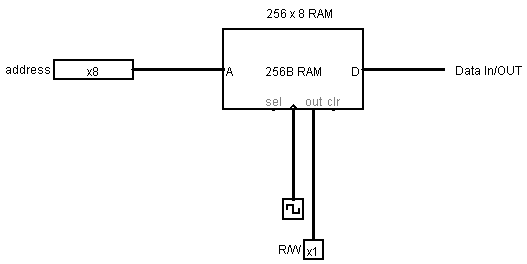
A 256 x 8 RAM consists of 256 8-bit cells (registers).
Each cell has a unique 8-bit address.
An 8-bit address input selects a cell.
A 1-bit R/W input selects an operation:
0 = WRITE
1 = READ
During a READ operation the content of the selected cell is copied to the 8-bit data port.
During a WRITE operation the 8-bit data port is interpreted as an input. During a clock pulse the value is copied into the selected cell.
Memory Interface Unit (MIU)
How can the data port of a RAM be both an input and an output port?
To solve this problem we create an MIU:
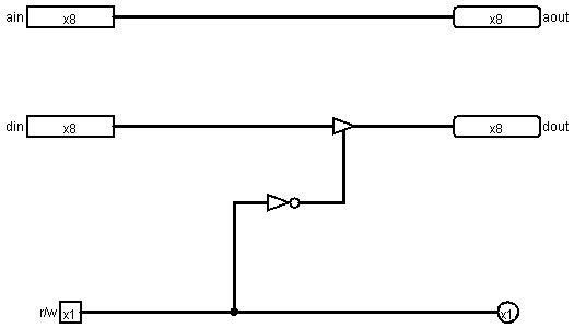
This simple circuit features a controlled buffer. When enabled, the output of this buffer is the same as its input. When disabled, the output floats. This means there is no output.
Notice that when the r/w input is 1 (READ), then the controlled buffer is disabled.
Simple Computer 1
Create a computer with a 4 x 8 data path, an MIU, an 8 bit IR, and a 256 x 8 RAM.
The binary format of IR:
000RDDAA
where
R = 0 (write) or 1 (read)
AA = address register
DD = data register
Simple Computer 2
Extend simple computer 1 with an ALU that can perform + and -.
Binary format of IR:
0oPPDDAA
where:
if (PP == 00) reg[DD] = reg[DD] + reg[AA]
if (PP = 01) reg[DD] = reg[DD] – reg[AA]
if (PP == 10) reg[DD]= RAM[reg[AA]]
if (PP == 11) RAM[reg[AA]] = reg[DD]
Here's a start: